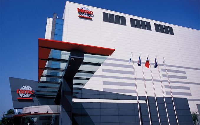
TSMC to Receive $6.6B Under US CHIPS Act, Set to Build 2nm Fab in Arizona
by Anton Shilov on April 8, 2024 4:30 PM EST- Posted in
- Semiconductors
- TSMC
- 5nm
- 3nm
- 4nm
- 2nm
- N2
- N3
- N4
- CHIPS & Science Act
TSMC has entered into a preliminary agreement with the U.S. Department of Commerce, securing up to $6.6 billion in direct funding and access to up to $5 billion in loans under the CHIPS and Science Act. With this latest round of support from the U.S. government, TSMC in turn will be adding a third fab to their Arizona project, with its investment in the region soaring to more than $65 billion. This move not only signifies the largest foreign direct investment in Arizona but also marks one of the biggest support packages that the U.S. government plans to make under the CHIPS Act, second only to Intel's $8.5 billion award last month.
TSMC is currently equipping its Fab 21 phase 1 and expects that it will start making chips using N4 and N5 (4 nm and 5 nm-class) process technologies in the first half of 2025. TSMC's Fab 21 phase 2 will commence operations in 2028, and will make chips on N3 and N2 (3 nm and 2 nm-class) production nodes. The newly-announced third fab (designation TBD) is set to manufacture chips on processes of 2 nm-class or beyond, with the start of production anticipated by the end of the decade.
TSMC has not announced a planned capacity for the new fab, only noting that it will be similar to the other two Arizona fabs, boasting a cleanroom space roughly twice as large as that of a typical "industry-standard logic fab." If it is sized similarly to the other Arizona fabs, then this strongly implies that the new fab will be another MegaFab-class facility – a mid-range fab producing around 25,000 wafer starts per month. TSMC does operate even larger fabs – the 100K WSPM GigaFab – though to date they've yet to build any of these outside of Taiwan.
“The CHIPS and Science Act provides TSMC the opportunity to make this unprecedented investment and to offer our foundry service of the most advanced manufacturing technologies in the United States,” said TSMC Chairman Dr. Mark Liu. “Our U.S. operations allow us to better support our U.S. customers, which include several of the world’s leading technology companies. Our U.S. operations will also expand our capability to trailblaze future advancements in semiconductor technology.”
The construction of three fabs in Arizona is poised to generate approximately 6,000 direct high-tech jobs, contributing significantly to the creation of a skilled workforce. This workforce is expected to play a crucial role in fostering a dynamic and competitive global semiconductor ecosystem. Moreover, the project is projected to create over 20,000 construction jobs, in addition to spawning tens of thousands of indirect jobs related to suppliers and consumer services.
AMD, Apple, and NVIDIA fully support TSMC's project and all of them expressed interest in using TSMC's capacities in the U.S.
“Today’s announcement highlights the strong commitment from Secretary Raimondo and the entire administration to ensure the U.S. plays a central role creating a more geographically diverse and resilient semiconductor supply chain,” said AMD Chair and CEO Lisa Su. “TSMC has a long track record of providing the leading-edge manufacturing capabilities that have enabled AMD to focus on what we do best, designing high-performance chips that change the world. We are committed to our partnership with TSMC and look forward to building our most advanced chips in U.S.”
TSMC's ventures in Arizona have encountered obstacles, such as setbacks caused by labor shortages and doubts about the U.S. governmental funding. As a result, production at the second facility has been postponed from 2026 to 2028. Moreover, Bloomberg has reported that at least one supplier for TSMC has called off its intended project in Arizona, attributing the decision to challenges in securing a workforce. The address the workforce issues, the TSMC grant includes a $50 million allocation for training of the local workforce.


23 Comments
View All Comments
Threska - Monday, April 8, 2024 - link
Fortunately no earthquakes to drive up costs. ReplyOxford Guy - Monday, April 8, 2024 - link
Its a good thing these things don't need water. ReplyBlastdoor - Tuesday, April 9, 2024 - link
Fabs are like swimming pools. You fill them up and then the water is re-used over and over.Also, this would be a far better use of water than the other stupid things done with water in Arizona. Massive amounts of water are wasted in Arizona to grow alfalfa for the Saudis. Just stop that massive waste and take a tiny fraction of that water for fabs. Reply
Jedi2155 - Wednesday, April 24, 2024 - link
There are also an astounding number of green golf courses in Arizona. Last time I flew over Phoenix, all the green I saw were basically for Golf. Replymeacupla - Monday, April 8, 2024 - link
TSMC Arizona fab is in a wildfire zone.The surrounding cities have various degrees of wildfire, flooding, and drought issues. Reply
Jedi2155 - Wednesday, April 24, 2024 - link
Wildfire is mainly an issue for the WUI (Wildland Urban Interface) which I don't think have a tremendous impact for the factory locations. Power shutoffs is for the lines that traverse these areas which I hope is mitigated as part of the planning. ReplyGeoffreyA - Tuesday, April 9, 2024 - link
Very fortunate indeed. Replytafreire - Monday, April 8, 2024 - link
It's still very little money if the US wants to become the largest chip producer in the world. Replytafreire - Monday, April 8, 2024 - link
A modern chip factory costs much more than US$6 billion. ReplyRedGreenBlue - Monday, April 8, 2024 - link
I think they previously got another 5 billion that was either a grant or a loan, news reports say different things. But they can apply for up to 25% of the 65 billion as a tax credit from the treasury so it makes it very appealing. Plus, TSMC wants to diversify their political and war risk. Hence, why they were set for building a fab in Japan in addition before this, and Japan is a NATO member. Reply